

Introduction
In 1965, Gordon Moore[Moor65] observed the doubling of processing power every year. Ever since, electronics industry has been driven forward by this (economical) law making it a self-fulfilling prophecy. The exponential growth in processing power has been made possible by producing ever smaller devices. This progress, with regard to further miniaturization, is steadily arriving at its ultimate and final limit: devices of atomic sizes connected by atomic wires.[Kurz01] Next to being of interest from the industrial point of view, nanowires are also important at the fundamental theoretical level because of their inherent one-dimensional (1D) nature. 1D electronic systems present exotic physical phenomena such as Peierls instability, charge density waves and Luttinger liquid behavior. Also dimensionality effects on, for example, magnetism and electronic properties can be studied in such systems.
Nanowires can be created in many different ways, resulting in a broad range of sizes, shapes and physical properties. This goes from break junction created monatomic gold wires to nanowires grown on imprinted surfaces; from atomic chains build one atom at a time using an STM tip to atomic Co chains grown on Pt(997) step edges and onward to self-assembled wires and stripes.
The variety in structures is huge and equaled by the variety of physical and chemical properties of these structures. Because of its high conductance gold is a favored metal used in the creation of atomic wires, both as free hanging wires and as reconstructed wires, chains or stripes on semiconductor surfaces.
Experimental Background
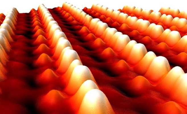
Figure 1: Pt Nanowires on Ge(001), on the cover of PRL.[Once05]
In 2003, Gürlü et al.[Gurl03] observed arrays of self-assembled nanowires by depositing a quarter monolayer of platinum (Pt) on a germanium(001)-surface and annealing it at over 1050K. They noticed that these nanowires only grow on a reconstructed germanium (Ge) surface which they call a β-terrace. Furthermore, the nanowires only appear in the troughs between the (quasi)-dimer-rows of these β-terraces. They are defect and kink free and their size is limited only by the size of the underlying β-terrace.
They suggested a tentative model, showing a β-terrace containing 0.25ML of Pt in its top-layer and a Pt-nanowire every second trough as can be seen in figure 1.
The bulges on the side of the nanowire are considered to be Pt atoms or pushed up Ge atoms. And there is at least one empty trough between the nanowires. This model was solely based on high resolution STM images, so some questions remain:
- Since STM is chemically insensitive, the position of the Pt atoms remains unknown.
- How much platinum is actually present in the different patches? 0.25ML was deposited for the entire sample, but this distribution is not perfectly homogeneous. As a result local variations in Pt density are to be expected.
- Why are there only nanowires every second trough, in a patch of nanowires?
- Why is there no conduction on the wires, but is there conduction in between the wires?
To answer such questions, computational work at the atomic scale was required. This would allow for (theoretical) models to be compared experimental observations. Furthermore, to be able to study the possible 1D phenomena associated with 1D systems a thorough knowledge of the atomic scale geometry is indispensable.
Theoretical Work
To identify the structure of the β-terrace and the nanowires we did ab initio total energy calculations using VASP. Ab initio calculations are named this way because the do not contain any assumptions or fitting (in theory). One only uses natural constants, the Schrodinger equation (or a reformulated version thereof, in my case the Hohenberg-Kohn-Sham equations) and basic knowledge of the atomic species (their mass, and number of electrons). As may be expected, such calculations are rather computationally expensive (compared to force-field calculations), but they are also very accurate and require very little prior knowledge of the system you are investigating (atomic types, and a reasonable guess of the atomic positions). This makes them very well suited for the modeling work at hand. The work-flow for the computations for this study is deceptively simple:
- Optimize the atomic positions in the model.
- Get the formation energy, and compare different models to find the ground state structure.
- Simulate STM images using the Tersoff-Hamann [Ters85] approach. Compare these simulated STM-pictures to experimental STM-pictures.
- Find nice correlation between best formation energies, and best fitting STM simulation.
- The End.
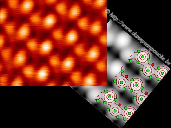
Figure 2: Comparison of the simulated (greyscale) STM image of the β6-structure to the experimental (redscale) STM image of a β-terrace. [1–3]
Unfortunately, computational work is never that simple. The main premise of point (i) is that we have a more-or-less correct model to start from. This premise, however, ended up to be false, resulting in a rather interesting search for the correct model of the Pt-nanowires on Ge(001).
β-terrace.
My calculations[1–3] showed many of the possible configurations containing a quarter monolayer of Pt in the top layer to be nearly degenerate in regard to their formation energy. This meant all structures should be equally accessible due to thermal motion. Comparison of simulated STM images of these structures to experimental images gave only good agreement for one structure when compared to large patches of defect free β-terrace. This reconstruction, the β6 structure,[3] contains a quarter monolayer of Pt in its top layer, giving rise to a checkerboard pattern of Ge-Ge and Pt-Ge dimers (cf. Fig. 2).
Nanowires.
Once a model for the β-terrace, corroborating the experimental observations, was found, our next goal became modeling the nanowires themself. Here, two possible scenarios can be imagined.
In the first one, the Pt atoms of the β-terrace are kicked out of the top layer of the β-terrace, during the annealing step, which reconstructs again to a normal Ge(001) surface. The expelled Pt atoms are then expected to form the nanowire.
A second scenario consists of extra Pt atoms forming the NW on top of the β-terrace. The additional Pt atoms would be provided by Pt which previously diffused deep into the substrate, and is ejected onto the surface during an anneal step. As such, the two scenarios are rather similar, their main difference being the original location of the ejected Pt atoms forming the experimentally observed nanowires.
Unfortunately, calculations for both scenarios showed that Pt nanowires are unstable in varying degrees. Furthermore, the calculated STM images show no agreement with the experimental images. As a result, a new model was required. The calculated STM images, next to being a final touchstone for our structures, were also vital in the process of constructing such a new model.
By using the image-signatures observed in the calculated STM images and their accompanying geometries as building blocks it was possible to construct a good model for the nanowires in an iterative fashion. The way of working used, shows some resemblance to a genetic algorithm:
- Generate/get/find a set of initial models.
- For a set of models simulate their STM images.
- If the simulated STM images match the experimentally observed images perfectly, go to 7, else go to 4.
- Compare the STM images of this generation of models to experimental STM images of the system.
- Use the underlying atomic structures of features observed in both simulation and experiment to generate a new set of models.
- Go back to 2.
- If it walks like a duck, talks like a duck, it must be a duck. You now have a good model for your system.

Figure 3: Simulated STM image of the Pt-induced nanowires on the Ge(001) surface. Green discs indicate the atomic positions of the bulk-Ge atoms; red: Pt atoms embedded in the top surface layers; yellow: Ge atoms forming the nanowire observed by STM.[1,2,4]
The main reasons the above algorithm could not be automated are the computational cost of doing density-functional theory (DFT) calculations on such large systems and points 4 and 5. Regarding the former, it is well doable to run through a few dozen to a hundred of such systems over a period of a few year, using modest TIER-2 facilities, a few thousand or tens of thousands is with current techniques is even on not-so-modest TIER-1 facilities an idle dream for a single (small) project. The latter point, however, is more difficult. Current day usage of genetic algorithms in computational materials design makes use of strict (and thus easy) selection criteria which are linked to absolute numbers (formation energy of a system, band-gap size, magnetization,…). In contrast, in this work the selection criterion sounded:”The simulated STM-images should look like those from experiments.” This is a rather vague and moves the focus from a quantitative to a qualitative nature. As a result, it becomes hard, if not impossible, to define a quantitative error.[7] Unlike computers, humans tend to be better at observing qualitative similarities, and do have a knack for recognizing patterns. As a result, managing points 4 and 5 consists mainly of manual labor.
This work took quite a bit of time due to the complexity of the system. However, in the end, we had a model which was both stable and gave calculated STM images that are in very good agreement with the observed experimental STM-images. Along the road to the final nanowire model, we also discovered (as byproducts) models for different reconstructions observed in the experiment during the nanowire-formation process.
The most remarkable result of this work is the discovery that the experimentally observed nanowires are actually Germanium nanowires (cf. Fig. 3).[1,4,8 ]This almost trivially explains the non-conducting nature of the observed nanowires, since they consist of a semi-conducting material.
CO adsorption on the Nanowires.
Because the nanwires were shown not to be conducting already early-on in their history, their nature was a point of unease. In addition, the perfection of the nanowires and the arrays of nanowires observed made them interesting systems to decorate with molecules within the context of molecular electronics. Experimental work by Oncel et al.[Once06] aimed at killing two birds with one stone. By using CO, adsorption on the nanowires would indicate them to consist of Pt (since the sticking affinity of CO is much larger on Pt than it is on Ge) and at the same time present the decoration of the nanowires with molecules opening the path to molecular electronics with this system. The experiments presented incredible results, the CO molecules were clearly observed to be linked to the nanowires, and furthermore, were seen to perform one-dimensional random walks along the nanowire attached to. Unfortunately, these results seem to be in stark contrast to our proposed model where the nanowire consists of Ge atoms.
Using the theoretical nanowire model I proposed, I investigated the adsorption of CO at different possible adsorption sites. The results, were also here quite amazing since they succeeded nicely in reconciling the nanowire model and the experimental observations.[5] Firstly, the adsorption of CO on Pt atoms embedded in the top layer of the surface was shown to be clearly favorable over CO adsorption on the Ge atoms of the nanowire. This is in agreement with what is known of their relative sticking affinities. Secondly, the CO molecules binding to the Pt atoms near the nanowire bend toward the nanowire.[5] As a result, the STM image of the CO molecules appears to be on the nanowire, albeit with a slight asymmetry. This asymmetry would mean that at least two types of CO-images should be observed in experiment (one leaning to one side of the nanowire, and one to the other side). This is in agreement with low temperature CO adsorption experiments.[Kock08]
")
Software
HIVE STM program: The Delphi program written for this project.
Related Publications
-
Phys. Rev. B 77, 241308(R) (2008),
doi: 10.1103/PhysRevB.77.241308 -
Mater. Res. Soc. Symp. Proc. 1177, 1177-Z03-09 (2009),
doi: 10.1557/PROC-1177-Z03-09 -
Phys. Rev. B 81, 035333 (2010),
doi: 10.1103/PhysRevB.81.035333 -
Phys. Rev. B 81, 085410 (2010),
doi: 10.1103/PhysRevB.81.085410 -
Phys. Rev. B 81, 235434 (2010),
doi: 10.1103/PhysRevB.81.235434 -
Belgian Physical Society Magazine 3, 11-16 (2011), (Featured Article for the BΦ)
-
Statistica Neerlandica 66, 339-355 (2012),
doi: 10.1111/j.1467-9574.2011.00519.x -
J. Phys.: Condens. Matter 26(13), 133001 (2014),
doi: 10.1088/0953-8984/26/13/133001
References
[Gurl03]
Appl. Phys. Lett. 83, 4610 (2003),doi: 10.1063/1.1630383
[Kock08]
Phys. Rev. B 78, 245421 (2008), doi: 10.1103/PhysRevB.78.245421
[Kurz01]
[Moor65]
[Once05]
Phys. Rev. Lett. 95, 116801 (2005), doi: 10.1103/PhysRevLett.95.116801
[Once06]
Surf. Sci. 600, 4690 (2006), doi: 10.1016/j.susc.2006.07.055
[Ters85]
Phys. Rev. B 31, 805 (1985), doi: 10.1103/PhysRevB.31.805