Tag: Low Dimensional Physics

Quasi-1D physics in metal-organic frameworks: MIL-47(V) from first principles

Authors: Danny E. P. Vanpoucke, Jan W. Jaeken, Stijn De Baerdemacker, Kurt Lejaeghere
and Veronique Van Speybroeck
Journal: Beilstein J. Nanotechnol. 5, 1738-1748 (2014)
doi: 10.3762/bjnano.5.184
IF(2014): 2.670
export: bibtex
pdf: <Beilstein> (open access)
Graphical Abstract: (left) Spin density of anti-ferromagnetic MIL-47(V) with ferromagnetic chains. (right) Electronic band structure and density of states.
Graphical Abstract: The MIL-47(V) MOF has one unpaired electron per V site. As a result, different spin configurations are possible, several of which lead to an anti-ferromagnetic state. The spin density of an antiferromagnetic state, containing only ferromagnetic chains is shown on the left. On the right, the electronic band structure of the same system is presented.

Abstract

The geometric and electronic structure of the MIL-47(V) metal-organic framework (MOF) is investigated by using ab initio density functional theory (DFT) calculations. Special focus is placed on the relation between the spin configuration and the properties of the MOF. The ground state is found to be antiferromagnetic, with an equilibrium volume of 1554.70 Å3. The transition pressure of the pressure-induced large-pore-to-narrow-pore phase transition is calculated to be 82 MPa and 124 MPa for systems with ferromagnetic and antiferromagnetic chains, respectively. For a mixed system, the transition pressure is found to be a weighted average of the ferromagnetic and antiferromagnetic transition pressures. Mapping DFT energies onto a simple-spin Hamiltonian shows both the intra- and inter-chain coupling to be antiferromagnetic, with the latter coupling constant being two orders of magnitude smaller than the former, suggesting the MIL-47(V) to present quasi-1D behavior. The electronic structure of the different spin configurations is investigated and it shows that the band gap position varies strongly with the spin configuration. The valence and conduction bands show a clear V d-character. In addition, these bands are flat in directions orthogonal to VO6 chains, while showing dispersion along the the direction of the VO6 chains, similar as for other quasi-1D materials.

Modeling 1D structures on semiconductor surfaces: Synergy of theory and experiment

Authors: Danny E. P. Vanpoucke
Journal: J. Phys.: Condens. Matter 26(13), 133001 (2014)
doi: 10.1088/0953-8984/26/13/133001
IF(2014): 2.346
export: bibtex
pdf: <J.Phys.Condens.Matter> <arXiv>

Abstract

Atomic scale nanowires attract enormous interest in a wide range of fields. On the one hand, due to their quasi-one-dimensional nature, they can act as an experimental testbed for exotic physics: Peierls instability, charge density waves, and Luttinger liquid behavior. On the other hand, due to their small size, they are of interest not only for future device applications in the micro-electronics industry, but also for applications regarding molecular electronics. This versatile nature makes them interesting systems to produce and study, but their size and growth conditions push both experimental production and theoretical modeling to their limits. In this review, modeling of atomic scale nanowires on semiconductor surfaces is discussed, focusing on the interplay between theory and experiment. The current state of modeling efforts on Pt- and Au-induced nanowires on Ge(001) is presented, indicating their similarities and differences. Recently discovered nanowire systems (Ir, Co, Sr) on the Ge(001) surface are also touched upon. The importance of scanning tunneling microscopy as a tool for direct comparison of theoretical and experimental data is shown, as is the power of density functional theory as an atomistic simulation approach. It becomes clear that complementary strengths of theoretical and experimental investigations are required for successful modeling of the atomistic nanowires, due to their complexity.

Pt Nanowires on Ge(001): Sheep in Wolf’s Clothing?

Authors: Danny E. P. Vanpoucke
Journal: Belgian Physical Society Magazine 3, 11-16 (2011)
(Featured Article for the BΦ)
pdf: <local>

Abstract

The deposition of small amounts of platinum on a germanium (001) surface gives rise to the formation of monatomic nanowires. These nanowires are defect–and kink-free and their length is only limited by the underlying terrace, to which they are uniquely connected. Using ab initio calculations and simulated scanning tunneling microscopy (STM) images we model these nanowires, and show them to consist of germanium atoms, in contrast to earlier proposed models.

CO adsorption on Pt-induced Ge nanowires

Authors: Danny E. P. Vanpoucke and Geert Brocks
Journal: Phys. Rev. B 81, 235434 (2010)
doi: 10.1103/PhysRevB.81.235434
IF(2010): 3.774
export: bibtex
pdf: <Phys.Rev.B> <arXiv>

Abstract

Using density-functional theory, we investigate the possible adsorption sites of CO molecules on the recently discovered Pt-induced Ge nanowires (NWs) on Ge(001). Calculated scanning tunneling microscope (STM) images are compared to experimental STM images to identify the experimentally observed adsorption sites. The CO molecules are found to adsorb preferably onto the Pt atoms between the Ge nanowire dimer segments. This adsorption site places the CO molecule in between two nanowire dimers, pushing them outward along the NW direction, blocking the nearest equivalent adsorption sites. This explains the observed long-range repulsive interaction between CO molecules on these Pt-induced nanowires.

Pt-induced nanowires on Ge(001): A density functional theory study

Authors: Danny E. P. Vanpoucke and Geert Brocks
Journal: Phys. Rev. B 81, 085410 (2010)
doi: 10.1103/PhysRevB.81.085410
IF(2010): 3.774
export: bibtex
pdf: <Phys.Rev.B> <arXiv>

Abstract

We study formation of the nanowires formed after deposition of Pt on a Ge(001) surface. The nanowires form spontaneously after high-temperature annealing. They are thermodynamically stable, only one atom wide and up to a few hundred atoms long. Ab initio density functional theory calculations are performed to identify possible structures of the Pt-Ge(001) surface with nanowires on top. A large number of structures are studied. With nanowires that are formed out of Pt or Ge dimers or mixed Pt-Ge dimers. By comparing simulated scanning tunneling microscopy images (STM) with experimental ones we model the formation of the nanowires and identify the geometries of the different phases in the formation process. We find that the formation of nanowires on a Pt-Ge(001) surface is a complex process based on increasing the Pt density in the top layers of the Ge(001) surface. Most remarkably we find the nanowires to consist of germanium dimers placed in troughs lined by mixed Pt-Ge dimer rows.

Ab Initio study of Pt Induced Nanowires on Ge(001)

Authors: Danny E.P. Vanpoucke
Ph.D. Thesis at University of Twente, The Netherlands
date: September 11th, 2009
Promoters Prof. Dr. Paul J. Kelly and Dr. Geert H. L. A. Brocks
doi: 10.3990/1.9789036528733
ISBN: 978-90-365-2873-3
#pages 193
export: bibtex
pdf: <PhD.Thesis> <UTwente>
research page with more information

Abstract

The aim of this thesis: “Ab Initio Study of Pt Induced Nanowires on Ge(001)”, is to model the experimentally observed ‘Pt nanowires’ on Ge(001). These one-atom-thick wires can be hundreds of nanometers long while remaining defect and kink free, providing the ultimate wire any chip designer dreams of. However, experiments show the wires not to be conducting; on the contrary, one-dimensional states are discovered between the wires. To model these nanowires, we combine state of the art density functional calculations with calculated scanning tunneling microscope (STM) images. First, the β-terrace substrate is modeled, showing a checkerboard pattern of Pt-Ge and Ge-Ge surface dimers in a Ge(001)-reconstructed surface.

Starting from this substrate model, different models with increasing Pt density are developed in an iterative fashion showing increasing agreement with the experimentally observed nanowires. We show that, contrary to previous assumptions, the observed wires are not Pt atoms but Ge atoms, explaining the lacking conductivity. The germanium nanowires consist of Ge dimers located in a Pt-lined trough. In addition, the 4×1 periodicity observed in the nanowire-arrays is traced back to the bonds of the Ge nanowire dimers to an extra Pt atom at the bottom of the trough, resulting in the buckling of the nanowires dimers.

In the last part of the thesis we investigate the adsorption of CO on the Ge nanowires under study. The observed adsorption of CO seems to contradict our proposed model due to the high sticking probability of CO on Pt, where it is low on Ge. We show that no contradiction exists. The CO molecules bind to the Pt atoms in the surface, but because they are tilted toward the nanowires, the resulting STM images give the impression that they are located on top of the nanowire giving rise to the apparent contradiction. In this last study, we also discover a very stable CO adsorption configuration in which the CO molecules remain invisible for STM, but could allow for the formation of one-dimensional molecular chains. This would open the door to one-dimensional molecular electronics.

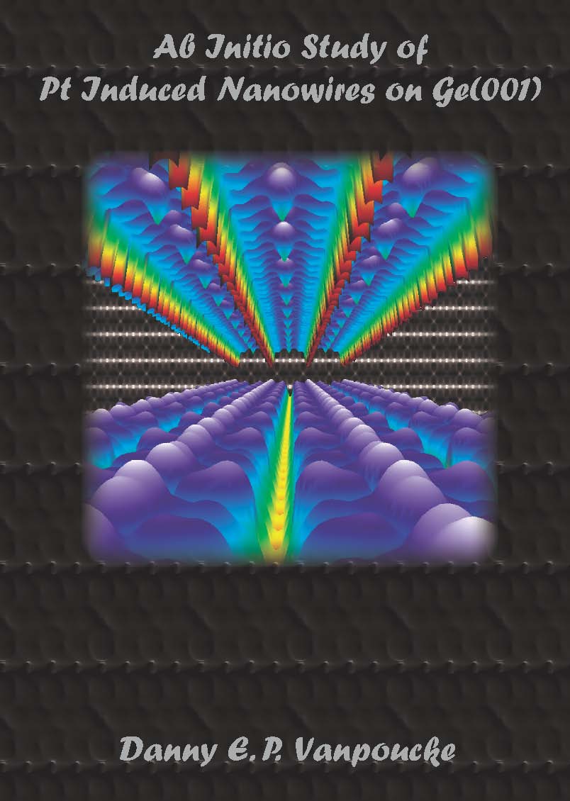
Front cover of the PhD thesis.

The formation of Self-Assembled Nanowire Arrays on Ge(001): a DFT study of Pt Induced Nanowire Arrays

Authors: Danny E. P. Vanpoucke and Geert Brocks
Book title: Symposium Z–Computational Nanoscience–How to Exploit Synergy between Predictive Simulations and Experiment
proceeding: Mater. Res. Soc. Symp. Proc. 1177, 1177-Z03-09 (2009)
doi: 10.1557/PROC-1177-Z03-09
export: bibtex
pdf: <MRS Proceeding> <arXiv>

Abstract

Nanowire (NW) arrays form spontaneously after high temperature annealing of a sub monolayer deposition of Pt on a Ge(001) surface. These NWs are a single atom wide, with a length limited only by the underlying beta-terrace to which they are uniquely connected. Using ab-initio density functional theory (DFT) calculations we study possible geometries of the NWs and substrate. Direct comparison to experiment is made via calculated scanning tunneling microscope (STM) images. Based on these images, geometries for the beta-terrace and the NWs are identified, and a formation path for the nanowires as function of increasing local Pt density is presented. We show the beta-terrace to be a dimer row surface reconstruction with a checkerboard pattern of Ge-Ge and Pt-Ge dimers. Most remarkably, comparison of calculated to experimental STM images shows the NWs to consist of germanium atoms embedded in the Pt-lined troughs of the underlying surface, contrary to what was assumed previously in experiments.

Formation of Pt-induced Ge atomic nanowires on Pt/Ge(001): A density functional theory study

Authors: Danny E. P. Vanpoucke and Geert Brocks
Journal: Phys. Rev. B 77, 241308 (2008)
doi: 10.1103/PhysRevB.77.241308
IF(2008): 3.322
export: bibtex
pdf: <Phys.Rev.B> <arXiv> <UTwentePublications>

Abstract

Pt deposited onto a Ge(001) surface gives rise to the spontaneous formation of atomic nanowires on a mixed Pt-Ge surface after high-temperature annealing. We study possible structures of the mixed surface and the nanowires by total energy density functional theory calculations. Experimental scanning-tunneling microscopy images are compared to the calculated local densities of states. On the basis of this comparison and the stability of the structures, we conclude that the formation of nanowires is driven by an increased concentration of Pt atoms in the Ge surface layers. Surprisingly, the atomic nanowires consist of Ge instead of Pt atoms.