Tag: PhD thesis 1

Slow science: the case of Pt induced nanowires on Ge(001)

Free-standing Pt-induced nanowire on Ge(001).

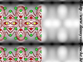
Simulated STM image of the Pt-induced nanowires on the Ge(001) surface. Green discs indicate the atomic positions of the bulk-Ge atoms; red: Pt atoms embedded in the top surface layers; yellow: Ge atoms forming the nanowire observed by STM.

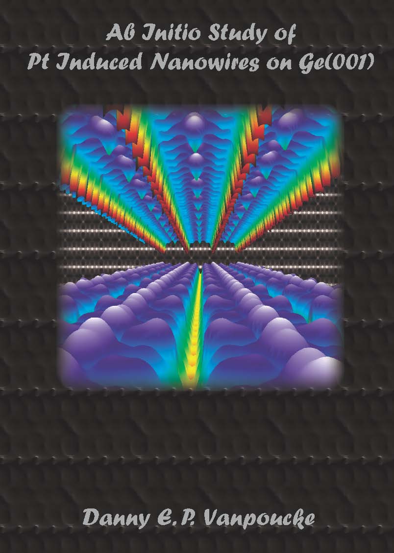
Ten years ago, I was happily modeling Pt nanowires on Ge(001) during my first Ph.D. at the university of Twente. As a member of the Computational Materials Science group, I also was lucky to have good and open contact with the experimental research group of Prof. Zandvliet, whom was growing these nanowires. In this environment, I learned there is a big difference between what is easy in experiment and what is easy in computational research. It also taught me to find a common ground which is “easy” for both (Scanning tunneling microscopy (STM) images in this specific case).

During this 4-year project, I quickly came to the conclusion that the nanowires could not be formed by Pt atoms, but that it needed to be Ge atoms instead. Although the simulated STM images were  very convincing, it was really hard to overcome the experimental intuition…and experiments which seemed to contradict this picture (doi: 10.1016/j.susc.2006.07.055 ). As a result, I spend a lot of time learning about the practical aspects of the experiments (an STM tip is a complicated thing) and trying to extract every possible piece of information published and unpublished. Especially the latter provided important support. The “ugly”(=not good for publishing) experimental pictures tended to be real treasures from my computational point of view. Of course, much time was spent on tweaking the computational model to get a perfect match with experiments (e.g. the 4×1 periodicity), and trying to reproduce experiments seemingly supporting the “Ge-nanowire” model (e.g. simulation of CO adsorption and identification of the path along the wire the molecule follows.).

In contrast to my optimism at the end of my first year (I believed all modeling could be finished before my second year ended), the modeling work ended up being a very complex exercise, taking 4 years of research. Now I am happy that I was wrong, as the final result ended up being very robust and became “The model for Pt induced nanowires on Ge(001)“.

Upon doing a review article on this field five years after my Ph.D. I was amazed (and happy) to see my model still stood. Even more, there had been complex experimental studies (doi: 10.1103/PhysRevB.85.245438) which even seemed to support the model I proposed. However, these experiments were stil making an indirect comparison. A direct comparison supporting the Ge nature of the nanowires was still missing…until recently.

In a recent paper in Phys. Rev. B (doi: 10.1103/PhysRevB.96.155415) a Japanese-Turkish collaboration succeeded in identifying the nanowire atoms as Ge atoms. They did this using an Atomic Force Microscope (AFM) and a sample of Pt induced nanowires, in which some of the nanowire atoms were replaced by Sn atoms. The experiment rather simple in idea (execution however requires rather advanced skills): compare the forces experienced by the AFM when measuring the Sn atom, the chain atoms and the surface atoms. The Sn atoms are easily recognized, while the surface is known to consist of Ge atoms. If the relative force of the chain atom is the same as that of the surface atoms, then the chain consists of Ge atoms, while if the force is different, the chain consists of Pt atoms.

*small drum-roll*

And they found the result to be the same.

Yes, after nearly 10 years since my first publication on the subject, there finally is experimental proof that the Pt nanowires on Ge(001) consist of Ge atoms. Seeing this paper made me one happy computational scientist. For me it shows the power of computational research, and provides an argument why one should not be shy to push calculations to their limit. The computational cost may be high, but at least one is performing relevant work. And of course, never forget, the most seemingly easy looking experiments are  usually not easy at all, so as a computational materials scientist you should not take them for granted, but let those experimentalists know how much you appreciate their work and effort.

CO adsorption on Pt-induced Ge nanowires

Authors: Danny E. P. Vanpoucke and Geert Brocks
Journal: Phys. Rev. B 81, 235434 (2010)
doi: 10.1103/PhysRevB.81.235434
IF(2010): 3.774
export: bibtex
pdf: <Phys.Rev.B> <arXiv>

Abstract

Using density-functional theory, we investigate the possible adsorption sites of CO molecules on the recently discovered Pt-induced Ge nanowires (NWs) on Ge(001). Calculated scanning tunneling microscope (STM) images are compared to experimental STM images to identify the experimentally observed adsorption sites. The CO molecules are found to adsorb preferably onto the Pt atoms between the Ge nanowire dimer segments. This adsorption site places the CO molecule in between two nanowire dimers, pushing them outward along the NW direction, blocking the nearest equivalent adsorption sites. This explains the observed long-range repulsive interaction between CO molecules on these Pt-induced nanowires.

Pt-induced nanowires on Ge(001): A density functional theory study

Authors: Danny E. P. Vanpoucke and Geert Brocks
Journal: Phys. Rev. B 81, 085410 (2010)
doi: 10.1103/PhysRevB.81.085410
IF(2010): 3.774
export: bibtex
pdf: <Phys.Rev.B> <arXiv>

Abstract

We study formation of the nanowires formed after deposition of Pt on a Ge(001) surface. The nanowires form spontaneously after high-temperature annealing. They are thermodynamically stable, only one atom wide and up to a few hundred atoms long. Ab initio density functional theory calculations are performed to identify possible structures of the Pt-Ge(001) surface with nanowires on top. A large number of structures are studied. With nanowires that are formed out of Pt or Ge dimers or mixed Pt-Ge dimers. By comparing simulated scanning tunneling microscopy images (STM) with experimental ones we model the formation of the nanowires and identify the geometries of the different phases in the formation process. We find that the formation of nanowires on a Pt-Ge(001) surface is a complex process based on increasing the Pt density in the top layers of the Ge(001) surface. Most remarkably we find the nanowires to consist of germanium dimers placed in troughs lined by mixed Pt-Ge dimer rows.

Density functional theory study of Pt-induced Ge(001) reconstructions

Authors: Danny E. P. Vanpoucke and Geert Brocks
Journal: Phys. Rev. B 81, 035333 (2010)
doi: 10.1103/PhysRevB.81.035333
IF(2010): 3.774
export: bibtex
pdf: <Phys.Rev.B> <arXiv>

Abstract

Pt deposited on a Ge(001) surface spontaneously forms nanowire arrays. These nanowires are thermodynamically stable and can be hundreds of atoms long. The nanowires only occur on a reconstructed Pt-Ge-surface where they fill the troughs between the dimer rows on the surface. This unique connection between the nanowires and the underlying substrate make a thorough understanding of the latter necessary for understanding the growth of the nanowires. In this paper we study possible surface reconstructions containing 0.25 and 0.5 of a monolayer of Pt. Comparison of calculated scanning tunneling microscope (STM) images to experimental STM images of the surface reconstruction reveal that the Pt atoms are located in the top layer, creating a structure with rows of alternating Pt-Ge and Ge-Ge dimers in a c(4×2) arrangement. Our results also show that Pt atoms in the second or third layer cannot be responsible for the experimentally observed STM images.

Ab Initio study of Pt Induced Nanowires on Ge(001)

Authors: Danny E.P. Vanpoucke
Ph.D. Thesis at University of Twente, The Netherlands
date: September 11th, 2009
Promoters Prof. Dr. Paul J. Kelly and Dr. Geert H. L. A. Brocks
doi: 10.3990/1.9789036528733
ISBN: 978-90-365-2873-3
#pages 193
export: bibtex
pdf: <PhD.Thesis> <UTwente>
research page with more information

Abstract

The aim of this thesis: “Ab Initio Study of Pt Induced Nanowires on Ge(001)”, is to model the experimentally observed ‘Pt nanowires’ on Ge(001). These one-atom-thick wires can be hundreds of nanometers long while remaining defect and kink free, providing the ultimate wire any chip designer dreams of. However, experiments show the wires not to be conducting; on the contrary, one-dimensional states are discovered between the wires. To model these nanowires, we combine state of the art density functional calculations with calculated scanning tunneling microscope (STM) images. First, the β-terrace substrate is modeled, showing a checkerboard pattern of Pt-Ge and Ge-Ge surface dimers in a Ge(001)-reconstructed surface.

Starting from this substrate model, different models with increasing Pt density are developed in an iterative fashion showing increasing agreement with the experimentally observed nanowires. We show that, contrary to previous assumptions, the observed wires are not Pt atoms but Ge atoms, explaining the lacking conductivity. The germanium nanowires consist of Ge dimers located in a Pt-lined trough. In addition, the 4×1 periodicity observed in the nanowire-arrays is traced back to the bonds of the Ge nanowire dimers to an extra Pt atom at the bottom of the trough, resulting in the buckling of the nanowires dimers.

In the last part of the thesis we investigate the adsorption of CO on the Ge nanowires under study. The observed adsorption of CO seems to contradict our proposed model due to the high sticking probability of CO on Pt, where it is low on Ge. We show that no contradiction exists. The CO molecules bind to the Pt atoms in the surface, but because they are tilted toward the nanowires, the resulting STM images give the impression that they are located on top of the nanowire giving rise to the apparent contradiction. In this last study, we also discover a very stable CO adsorption configuration in which the CO molecules remain invisible for STM, but could allow for the formation of one-dimensional molecular chains. This would open the door to one-dimensional molecular electronics.

Front cover of the PhD thesis.

The formation of Self-Assembled Nanowire Arrays on Ge(001): a DFT study of Pt Induced Nanowire Arrays

Authors: Danny E. P. Vanpoucke and Geert Brocks
Book title: Symposium Z–Computational Nanoscience–How to Exploit Synergy between Predictive Simulations and Experiment
proceeding: Mater. Res. Soc. Symp. Proc. 1177, 1177-Z03-09 (2009)
doi: 10.1557/PROC-1177-Z03-09
export: bibtex
pdf: <MRS Proceeding> <arXiv>

Abstract

Nanowire (NW) arrays form spontaneously after high temperature annealing of a sub monolayer deposition of Pt on a Ge(001) surface. These NWs are a single atom wide, with a length limited only by the underlying beta-terrace to which they are uniquely connected. Using ab-initio density functional theory (DFT) calculations we study possible geometries of the NWs and substrate. Direct comparison to experiment is made via calculated scanning tunneling microscope (STM) images. Based on these images, geometries for the beta-terrace and the NWs are identified, and a formation path for the nanowires as function of increasing local Pt density is presented. We show the beta-terrace to be a dimer row surface reconstruction with a checkerboard pattern of Ge-Ge and Pt-Ge dimers. Most remarkably, comparison of calculated to experimental STM images shows the NWs to consist of germanium atoms embedded in the Pt-lined troughs of the underlying surface, contrary to what was assumed previously in experiments.

Formation of Pt-induced Ge atomic nanowires on Pt/Ge(001): A density functional theory study

Authors: Danny E. P. Vanpoucke and Geert Brocks
Journal: Phys. Rev. B 77, 241308 (2008)
doi: 10.1103/PhysRevB.77.241308
IF(2008): 3.322
export: bibtex
pdf: <Phys.Rev.B> <arXiv> <UTwentePublications>

Abstract

Pt deposited onto a Ge(001) surface gives rise to the spontaneous formation of atomic nanowires on a mixed Pt-Ge surface after high-temperature annealing. We study possible structures of the mixed surface and the nanowires by total energy density functional theory calculations. Experimental scanning-tunneling microscopy images are compared to the calculated local densities of states. On the basis of this comparison and the stability of the structures, we conclude that the formation of nanowires is driven by an increased concentration of Pt atoms in the Ge surface layers. Surprisingly, the atomic nanowires consist of Ge instead of Pt atoms.