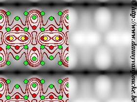
Simulated STM image of the Pt-induced nanowires on the Ge(001) surface. Green discs indicate the atomic positions of the bulk-Ge atoms; red: Pt atoms embedded in the top surface layers; yellow: Ge atoms forming the nanowire observed by STM.
Ten years ago, I was happily modeling Pt nanowires on Ge(001) during my first Ph.D. at the university of Twente. As a member of the Computational Materials Science group, I also was lucky to have good and open contact with the experimental research group of Prof. Zandvliet, whom was growing these nanowires. In this environment, I learned there is a big difference between what is easy in experiment and what is easy in computational research. It also taught me to find a common ground which is “easy” for both (Scanning tunneling microscopy (STM) images in this specific case).
During this 4-year project, I quickly came to the conclusion that the nanowires could not be formed by Pt atoms, but that it needed to be Ge atoms instead. Although the simulated STM images were very convincing, it was really hard to overcome the experimental intuition…and experiments which seemed to contradict this picture (doi: 10.1016/j.susc.2006.07.055 ). As a result, I spend a lot of time learning about the practical aspects of the experiments (an STM tip is a complicated thing) and trying to extract every possible piece of information published and unpublished. Especially the latter provided important support. The “ugly”(=not good for publishing) experimental pictures tended to be real treasures from my computational point of view. Of course, much time was spent on tweaking the computational model to get a perfect match with experiments (e.g. the 4×1 periodicity), and trying to reproduce experiments seemingly supporting the “Ge-nanowire” model (e.g. simulation of CO adsorption and identification of the path along the wire the molecule follows.).
In contrast to my optimism at the end of my first year (I believed all modeling could be finished before my second year ended), the modeling work ended up being a very complex exercise, taking 4 years of research. Now I am happy that I was wrong, as the final result ended up being very robust and became “The model for Pt induced nanowires on Ge(001)“.
Upon doing a review article on this field five years after my Ph.D. I was amazed (and happy) to see my model still stood. Even more, there had been complex experimental studies (doi: 10.1103/PhysRevB.85.245438) which even seemed to support the model I proposed. However, these experiments were stil making an indirect comparison. A direct comparison supporting the Ge nature of the nanowires was still missing…until recently.
In a recent paper in Phys. Rev. B (doi: 10.1103/PhysRevB.96.155415) a Japanese-Turkish collaboration succeeded in identifying the nanowire atoms as Ge atoms. They did this using an Atomic Force Microscope (AFM) and a sample of Pt induced nanowires, in which some of the nanowire atoms were replaced by Sn atoms. The experiment rather simple in idea (execution however requires rather advanced skills): compare the forces experienced by the AFM when measuring the Sn atom, the chain atoms and the surface atoms. The Sn atoms are easily recognized, while the surface is known to consist of Ge atoms. If the relative force of the chain atom is the same as that of the surface atoms, then the chain consists of Ge atoms, while if the force is different, the chain consists of Pt atoms.
*small drum-roll*
And they found the result to be the same.
Yes, after nearly 10 years since my first publication on the subject, there finally is experimental proof that the Pt nanowires on Ge(001) consist of Ge atoms. Seeing this paper made me one happy computational scientist. For me it shows the power of computational research, and provides an argument why one should not be shy to push calculations to their limit. The computational cost may be high, but at least one is performing relevant work. And of course, never forget, the most seemingly easy looking experiments are usually not easy at all, so as a computational materials scientist you should not take them for granted, but let those experimentalists know how much you appreciate their work and effort.

