It is a yearly habbit, the Hasselt diamond conference with the cryptic name SBDD. It stands for “Surface and Bulk Defects in Diamond”, though few remember as the accronym has been in common use for quite a while. This year, we celebrated the thirtied edition, or XXX using roman numerals. A celebratory edition which was filled with some special events, such as the XXX session (of course that was a fun group quize about the conference, what else did you think?), a caricaturist, a claw machine with SBDD goodies, a photobooth and a scientific poster/image competition. Indeed, the diamond community is a true scientific family when at SBDD.

SBDD XXX conference. Top left: Aylin Melan, Eleonora Thomas and Thijs van Wijk with the group poster. Top right: SBDD XXX poster prize winners. Bottom left: Caricature of Danny Vanpoucke on a beer coaster. Bottom right: Aylin with her prize winning poster.
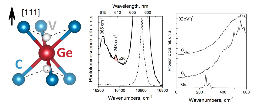
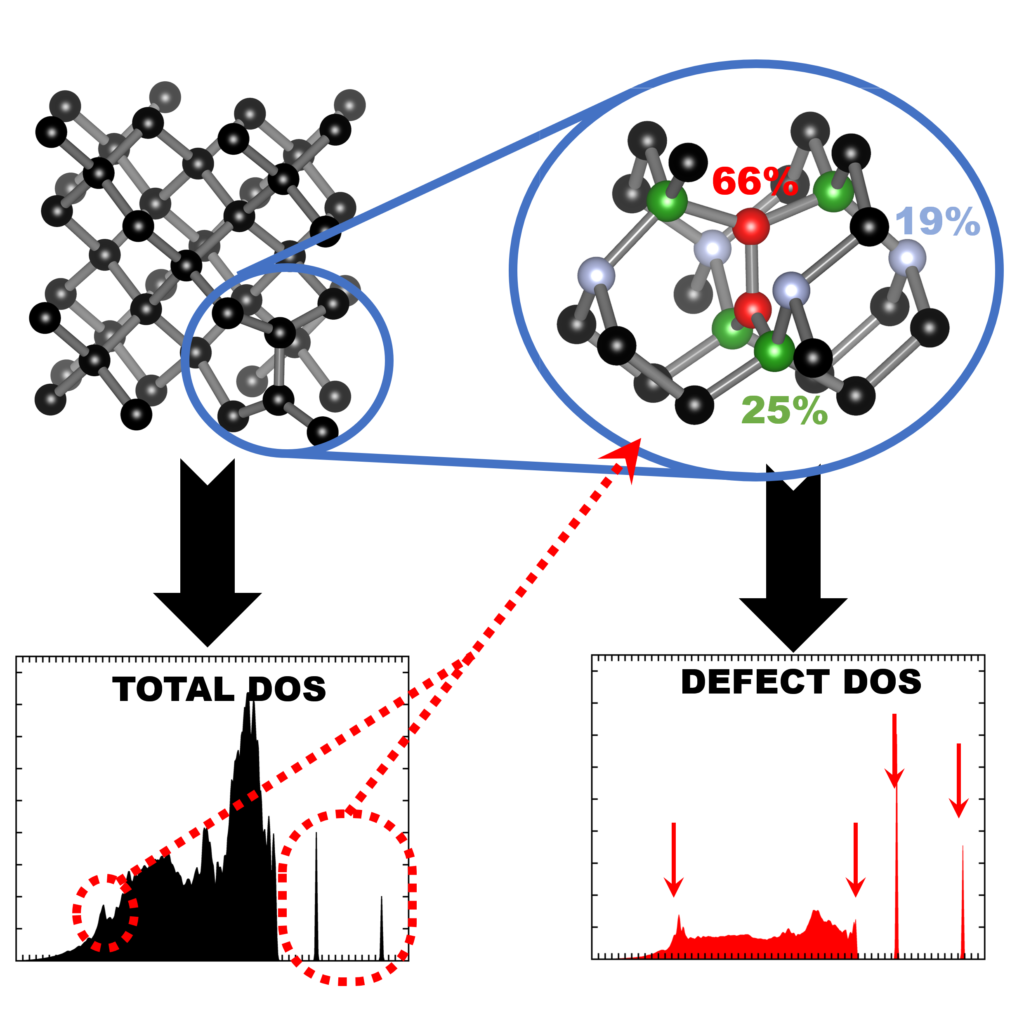
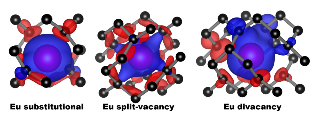
QuATOMs was present with no less than 3 posters, and this year there was also good company from other theoretical contributors. We presented posters focussing on group-IV defects in diamond as well as our ambitions for the future. There was a huge number of posters (>170), with a lot of interest in modeling of defects. Any conference with poster sessions, also has a posterprize competition. This year, I’m happy to share that Aylin Melan won a Brillian poster prize at SBDD for her theoretical poster on GeV color centers, because of her skills at explaining the topic clearly for a broad (experimental) audience, as well as having a very nice poster. Congratulations Aylin!

 During the last year,