Tag: theory and experiment

Science Figured out

Diamond and CPU's, now still separated, but how much longer will this remain the case? Top left: Thin film N-doped diamond on Si (courtesy of Sankaran Kamatchi). Top right: Very old Pentium 1 CPU from 1993 (100MHz), with µm architecture. Bottom left: more recent intel core CPU (3GHz) of 2006 with nm scale architecture. Bottom right: Piece of single crystal diamond. A possible alternative for silicon, with 20x higher thermal conductivity, and 7x higher mobility of charge carriers.

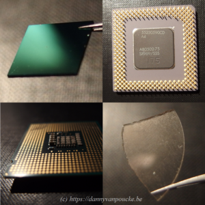
Diamond and CPU’s, now still separated, but how much longer will this remain the case?
Top left: Thin film N-doped diamond on Si (courtesy of Sankaran Kamatchi). Top right: Very old Pentium 1 CPU from 1993 (100MHz), with µm architecture. Bottom left: more recent intel core CPU (3GHz) of 2006 with nm scale architecture. Bottom right: Piece of single crystal diamond. A possible alternative for silicon, with 20x higher thermal conductivity, and 7x higher mobility of charge carriers.

Can you pitch your research in 3 minutes, this is the concept behind “wetenschap uitgedokterd/science figured out“. A challenge I accepted after the fun I had at the science-battle. If I can explain my work to a public of 6 to 12 year-olds, explaining it to adults should be possible as well. However, 3 minutes is very short (although some may consider this long in the current bitesize world), especially if you have to explain something far from day-to-day life and can not assume any scientific background.

Where to start? Capture the imagination: “Imagine a world where you are a god.

Link back to the real world. “All modern-day high-tech toys are more and more influenced by the atomic scale details.” Over the last decade, I have seen the nano-scale progress slowly but steadily into the realm of real-life materials research. This almost invisible trend will have a huge impact on materials science in the coming decade, because more and more we will see empirical laws breaking down, and it will become harder and harder to fit trends of materials using a classical mindset, something which has worked marvelously for materials science during the last few centuries. Modern and future materials design (be it solar cells, batteries, CPU’s or even medicine) will have to rely on quantum mechanical intuition and hence quantum mechanical simulations. (Although there is still much denial in that regard.)

Is there a problem to be solved? Yes indeed: “We do not have quantum mechanical intuition by nature, and manipulating atoms is extremely hard in practice and for practical purposes.” Although popular science magazines every so often boast pictures of atomic scale manipulation of atoms and the quantum regime, this makes it far from easy and common inside and outside the university lab. It is amazing how hard these things tend to get (ask your local experimental materials research PhD) and the required blood, sweat and tears are generally not represented in the glory-parade of a scientific publication.

Can you solve this? Euhm…yes…at least to some extend. “Computational materials research can provide the quantum mechanical intuition we human beings lack, and gives us access to atomic scale manipulation of a material.” Although computational materials science is seen by experimentalists as theory, and by theoreticians as experiments, it is neither and both. Computational materials science combines the rigor and control of theory, with access to real-life systems of experiments. It, unfortunately also suffers the limitations of both: as the system is still idealized (but to much lesser extend than in theoretical work) and control is not absolute (you have to follow where the algorithms take you, just as an experimentalist has to follow where the reaction takes him/her). But, if these strengths and weaknesses are balanced wisely (requires quite a few years of experience) an expert will gain fundamental insights in experiments.

Animation representing the buildup of a diamond surface in computational work.

Animation representing the buildup of a diamond surface in computational work.

As a computational materials scientist, you build a real-life system, atom by atom, such that you know exactly where everything is located, and then calculate its properties based on the rules of quantum mechanics, for example. In this sense you have absolute control as in theory. This comes at a cost (conservation of misery 🙂 ); where nature itself makes sure the structure is the “correct one” in experiments, you have to find it yourself in computational work. So you generally end up calculating many possible structural combinations of your atoms to first find out which is the one most probable to represent nature.
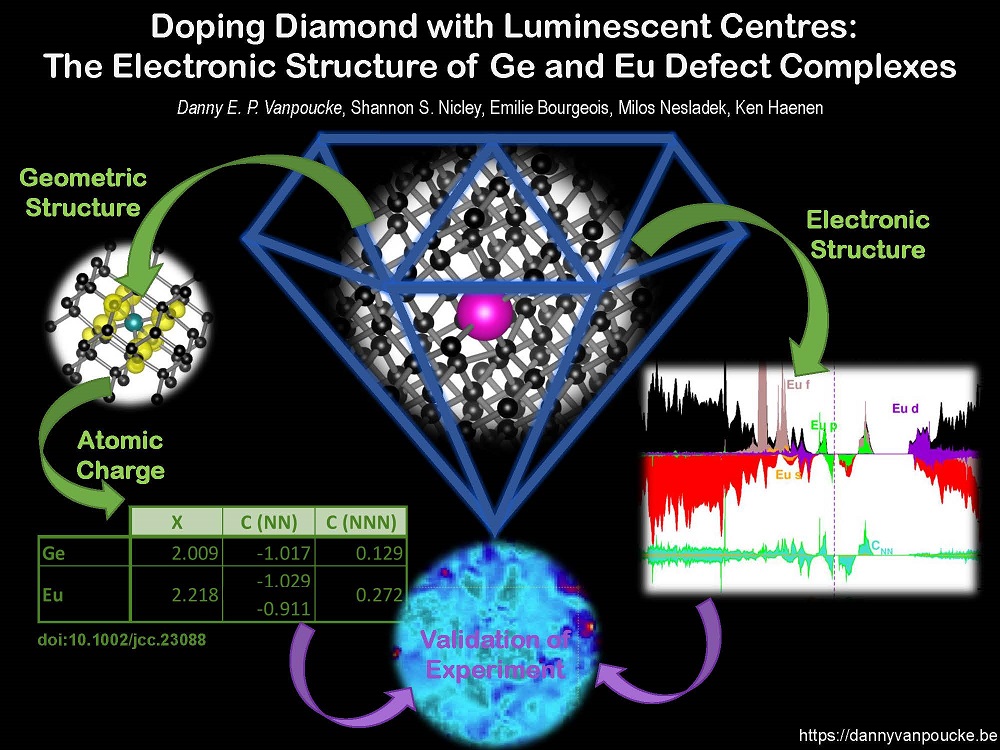
So what am I actually doing?I am using atomic scale quantum mechanical computations to investigate the materials my experimental colleagues are studying, going from oxides to defects in diamond.” I know this is vague, but unfortunately, the actual work is technical. Much effort goes into getting the calculations to run in the direction you want them to proceed (This is the experimental side of computational materials science.). The actual goal varies from project to project. Sometimes, we want to find out which material is most stable, and which material is most likely to diffuse into the other, while at other times we want to understand the electronic structure, to test if a defect is really luminescent, this to trace the source of the experimentally observed luminescence. Or if you want to make it more complex, even find out which elements would make diamond grow faster.

Starting from this, I succeeded in creating a 3-minute pitch of my research for Science Figured out. The pitch can be seen here (in Dutch, with English subtitles that can be switched on through the cogwheel in the bottom right corner).

Some external links:


VSC User Day 2018

Today, I am attending the 4th VSC User Day at the “Paleis de Academiën” in Brussels. Flemish researchers for whom the lifeblood of their research flows through the chips of a supercomputer are gathered here to discuss their experiences and present their research.

Some History

About 10 years ago, at the end of 2007 and beginning of 2008, the 5 Flemish universities founded the Flemish Supercomputer Center (VSC). A virtual organisation with one central goal:  Combine their strengths and know-how with regard to High Performance Compute (HPC) centers to make sure they were competitive with comparable HPC centers elsewhere.

By installing a super-fast network between the various university compute centers, each Flemish researcher has nowadays access to state-of-the-art computer infrastructure, independent of his or her physical location. A researcher at the University of Hasselt, like myself, can easily run calculations on the supercomputers installed at the university of Ghent or Leuven. In October 2012 the existing university supercomputers, so-called Tier-2 supercomputers, are joined by the first Flemish Tier-1 supercomputer, which was housed at the brand new data-centre of Ghent University. This machine is significantly larger than the existing Tier-2 machines, and allows Belgium to become the 25th member of the PRACE network, a European network which provides computational researchers access to the best and largest computer facilities in Europe. The fast development of computational research in Flanders and the explosive growth in the number of computational researchers, combined with the first shared Flemish supercomputer (in contrast to the university TIER-2 supercomputers, which some still consider private property rather than part of VSC) show the impact of the virtual organisation that is the VSC. As a result, on January 16th 2014, the first VSC User Day is organised, bringing together HPC users from all 5 universities  and industry. Here the users share their experiences and discuss possible improvements and changes. Since then, the first Tier-1 supercomputer has been decommissioned and replaced by a brand new Tier-1 machine, this time located at the KU Leuven. Furthermore, the Flemish government has put 30M€ aside for super-computing in Flanders, making sure that also in the future Flemish computational research stays competitive. The future of computational research in Flanders looks bright.

Today is User Day 2018

During the 4th VSC User Day, researchers of all 5 Flemish universities will be presenting the work they are performing on the supercomputers of the VSC network. The range of topics is very broad: from first principles materials modelling to chip design, climate modelling and space weather. In addition there will also be several workshops, introducing new users to the VSC and teaching advanced users the finer details of GPU-code and code optimization and parallelization. This later aspect is hugely important during the use of supercomputers in an academic context. Much of the software used is developed or modified by the researchers themselves. And even though this software can present impressive behavior, it doe not speed up automatically if you provide it access to more CPU’s. This is a very non-trivial task the researchers has to take care of, by carefully optimizing and parallelizing his or her code.

To support the researchers in their work, the VSC came up with ingenious poster-prizes. The three best posters will share 2018 node days of calculation time (about 155 years of calculations on a normal simple computer).

Wish me luck!


Single-slide presentation of my poster @VSC User Day 2018.

Single-slide presentation of my poster @VSC User Day 2018.

Slow science: the case of Pt induced nanowires on Ge(001)

Free-standing Pt-induced nanowire on Ge(001).

Simulated STM image of the Pt-induced nanowires on the Ge(001) surface. Green discs indicate the atomic positions of the bulk-Ge atoms; red: Pt atoms embedded in the top surface layers; yellow: Ge atoms forming the nanowire observed by STM.

Ten years ago, I was happily modeling Pt nanowires on Ge(001) during my first Ph.D. at the university of Twente. As a member of the Computational Materials Science group, I also was lucky to have good and open contact with the experimental research group of Prof. Zandvliet, whom was growing these nanowires. In this environment, I learned there is a big difference between what is easy in experiment and what is easy in computational research. It also taught me to find a common ground which is “easy” for both (Scanning tunneling microscopy (STM) images in this specific case).

During this 4-year project, I quickly came to the conclusion that the nanowires could not be formed by Pt atoms, but that it needed to be Ge atoms instead. Although the simulated STM images were  very convincing, it was really hard to overcome the experimental intuition…and experiments which seemed to contradict this picture (doi: 10.1016/j.susc.2006.07.055 ). As a result, I spend a lot of time learning about the practical aspects of the experiments (an STM tip is a complicated thing) and trying to extract every possible piece of information published and unpublished. Especially the latter provided important support. The “ugly”(=not good for publishing) experimental pictures tended to be real treasures from my computational point of view. Of course, much time was spent on tweaking the computational model to get a perfect match with experiments (e.g. the 4×1 periodicity), and trying to reproduce experiments seemingly supporting the “Ge-nanowire” model (e.g. simulation of CO adsorption and identification of the path along the wire the molecule follows.).

In contrast to my optimism at the end of my first year (I believed all modeling could be finished before my second year ended), the modeling work ended up being a very complex exercise, taking 4 years of research. Now I am happy that I was wrong, as the final result ended up being very robust and became “The model for Pt induced nanowires on Ge(001)“.

Upon doing a review article on this field five years after my Ph.D. I was amazed (and happy) to see my model still stood. Even more, there had been complex experimental studies (doi: 10.1103/PhysRevB.85.245438) which even seemed to support the model I proposed. However, these experiments were stil making an indirect comparison. A direct comparison supporting the Ge nature of the nanowires was still missing…until recently.

In a recent paper in Phys. Rev. B (doi: 10.1103/PhysRevB.96.155415) a Japanese-Turkish collaboration succeeded in identifying the nanowire atoms as Ge atoms. They did this using an Atomic Force Microscope (AFM) and a sample of Pt induced nanowires, in which some of the nanowire atoms were replaced by Sn atoms. The experiment rather simple in idea (execution however requires rather advanced skills): compare the forces experienced by the AFM when measuring the Sn atom, the chain atoms and the surface atoms. The Sn atoms are easily recognized, while the surface is known to consist of Ge atoms. If the relative force of the chain atom is the same as that of the surface atoms, then the chain consists of Ge atoms, while if the force is different, the chain consists of Pt atoms.

*small drum-roll*

And they found the result to be the same.

Yes, after nearly 10 years since my first publication on the subject, there finally is experimental proof that the Pt nanowires on Ge(001) consist of Ge atoms. Seeing this paper made me one happy computational scientist. For me it shows the power of computational research, and provides an argument why one should not be shy to push calculations to their limit. The computational cost may be high, but at least one is performing relevant work. And of course, never forget, the most seemingly easy looking experiments are  usually not easy at all, so as a computational materials scientist you should not take them for granted, but let those experimentalists know how much you appreciate their work and effort.

A combined experimental and theoretical investigation of the Al-Melamine reactive milling system: a mechanistic study towards AlN-based ceramics

Authors: Seyyed Amin Rounaghi, Danny E.P. Vanpoucke, Hossein Eshghi, Sergio Scudino, Elaheh Esmaeili, Steffen Oswald and Jürgen Eckert
Journal: J. Alloys Compd. 729, 240-248 (2017)
doi: 10.1016/j.jallcom.2017.09.168
IF(2017): 3.779
export: bibtex
pdf: <J.Alloys Compd.>


Graphical Abstract: Evolution of the end products as function of Al and N content during ball-milling synthesis of AlN.

Abstract

A versatile ball milling process was employed for the synthesis of hexagonal aluminum nitride (h-AlN) through the reaction of metallic aluminum with melamine. A combined experimental and theoretical study was carried out to evaluate the synthesized products. Milling intermediates and products were fully characterized via various techniques including XRD, FTIR, XPS, Raman and TEM. Moreover, a Boltzmann distribution model was proposed to investigate the effect of milling energy and reactant ratios on the thermodynamic stability and the proportion of different milling products. According to the results, the reaction mechanism and milling products were significantly influenced by the reactant ratio. The optimized condition for AlN synthesis was found to be at Al/M molar ratio of 6, where the final products were consisted of nanostructured AlN with average crystallite size of 11 nm and non-crystalline heterogeneous carbon.

Mechanochemical synthesis of nanostructured metal nitrides, carbonitrides and carbon nitride: A combined theoretical and experimental study

Authors: Seyyed Amin Rounaghi, Danny E.P. Vanpoucke, Hossein Eshghi, Sergio Scudino, Elaheh Esmaeili, Steffen Oswald and Jürgen Eckert
Journal: Phys. Chem. Chem. Phys. 19, 12414-12424 (2017)
doi: 10.1039/C7CP00998D
IF(2017): 3.906
export: bibtex
pdf: <Phys.Chem.Chem.Phys.>

Abstract

Nowadays, the development of highly efficient routes for the low cost synthesis of nitrides is greatly growing. Mechanochemical synthesis is one of those promising techniques which is conventionally employed for the synthesis of nitrides by long term milling of metallic elements under pressurized N2 or NH3 atmosphere (A. Calka and J. I. Nikolov, Nanostruct. Mater., 1995, 6, 409-412). In the present study, we describe a versatile, room-temperature and low cost mechanochemical process for the synthesis of nanostructured metal nitrides (MNs), carbonitrides (MCNs) and carbon nitride (CNx). Based on this technique, melamine as a solid nitrogen-containing organic compound (SNCOC) is ball milled with four different metal powders (Al, Ti, Cr and V) to produce nanostructured AlN, TiCxN1-x, CrCxN1-x, and VCxN1-x (x~0.05). Both theoretical and experimental techniques are implemented to determine the reaction intermediates, products, by-products and finally, the mechanism underling this synthetic route. According to the results, melamine is polymerized in the presence of metallic elements at intermediate stages of the milling process, leading to the formation of a carbon nitride network. The CNx phase subsequently reacts with the metallic precursors to form MN, MCN or even MCN-CNx nano-composites depending on the defect formation energy and thermodynamic stability of the corresponding metal nitride, carbide and C/N co-doped structures.

Call for Abstracts: Condensed Matter Science in Porous Frameworks: On Zeolites, Metal- and Covalent-Organic Frameworks

Flyer for the Colloquium on Porous Frameworks at the CMD26Together with Ionut Tranca (TU Eindhoven, The Netherlands) and Bartłomiej Szyja (Wrocław University of Technology, Poland) I am organizing a colloquium “Condensed Matter Science in Porous Frameworks: On Zeolites, Metal- and Covalent-Organic Frameworks” which will take place during the 26th biannual Conference & Exhibition CMD26 – Condensed Matter in Groningen (September 4th – 9th, 2016). During our colloquium, we hope to bring together experimental and theoretical researchers working in the field of porous frameworks, providing them the opportunity to present and discuss their latest work and discoveries.

Zeolites, Metal-Organic Frameworks, and Covalent-Organic Frameworks are an interesting class of hybrid materials. They are situated at the boundary of research fields, with properties akin to both molecules and solids. In addition, their porosity puts them at the boundary between surfaces and bulk materials, while their modular nature provides a wealthy playground for materials design.

We invite you to submit your abstract for oral or poster contributions to our colloquium. Poster contributions participate in a Best Poster Prize competition.

The deadline for abstract submission is April 30th, 2016.

The extended deadline for abstract submission is May 14th, 2016.


CMD26 – Condensed Matter in Groningen is an international conference, organized by the Condensed Matter Division of the European Physical Society, covering all aspects of condensed matter physics, including soft condensed matter, biophysics, materials science, quantum physics and quantum simulators, low temperature physics, quantum fluids, strongly correlated materials, semiconductor physics, magnetism, surface and interface physics, electronic, optical and structural properties of materials. The scientific programme will consist of a series of plenary and semi-plenary talks and Mini-colloquia. Within each Mini-colloquium, there will be invited lectures, oral contributions and posters.


Feel free to distribute this call for abstracts and our flyer and we hope to see you in Groningen!

Computational Materials Science: Where Theory Meets Experiments

Authors: Danny E. P. Vanpoucke,
Journal: Developments in Strategic Ceramic Materials:
Ceramic Engineering and Science Proceedings 36(8), 323-334 (2016)
(ICACC 2015 conference proceeding)
Editors: Waltraud M. Kriven, Jingyang Wang, Dongming Zhu,Thomas Fischer, Soshu Kirihara
ISBN: 978-1-119-21173-0
webpage: Wiley-VCH
export: bibtex
pdf: <preprint> 

Abstract

In contemporary materials research, we are able to create and manipulate materials at ever smaller scales: the growth of wires with nanoscale dimensions and the deposition of layers with a thickness of only a few atoms are just two examples that have become common practice. At this small scale, quantum mechanical effects become important, and this is where computational materials research comes into play. Using clever approximations, it is possible to simulate systems with a scale relevant for experiments. The resulting theoretical models provide fundamental insights in the underlying physics and chemistry, essential for advancing modern materials research. As a result, the use of computational experiments is rapidly becoming an important tool in materials research both for predictive modeling of new materials and for gaining fundamental insights in the behavior of existing materials. Computer and lab experiments have complementary limitations and strengths; only by combining them can the deepest fundamental secrets of a material be revealed.

In this paper, we discuss the application of computational materials science for nanowires on semiconductor surfaces, ceramic materials and flexible metal-organic frameworks, and how direct comparison can advance insight in the structure and properties of these materials.